EK-U1-VCU118-G
分類:Zynq
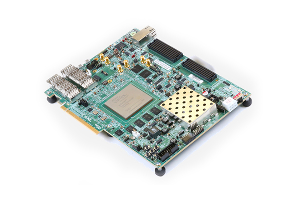
The Virtex® UltraScale+™ FPGA VCU118 Evaluation Kit is the ideal development environment for evaluating the cutting edge Virtex UltraScale+ FPGAs. Virtex UltraScale+ devices provide the highest performance and integration capabilities in a FinFET node, including both the highest serial I/O and signal processing bandwidth, as well as the highest on-chip memory density.
This kit is ideal for prototyping applications ranging from 1+ Tb/s networking and data center to fully integrated radar/early-warning systems.
- Dual 80-bit DDR4 Component Memory
- RLDRAM3 (2×36-bit) Memory
- Dual QSFP28 Interfaces
- PCIe Gen3 x16 (VCCINT = 0.85V)
- VITA 57.4 FMC+ Interface
- VITA 57.1 FMC Interface
- Samtec FireFly Interface
Configuration
- Onboard JTAG configuration circuitry to enable configuration over USB
- JTAG header provided for use with Xilinx download cables such as the Platform Cable USB II
- QSPI flash memory
Communication & Networking
- 10/100/1000 Mbps Ethernet (SGMII)
- Dual 4x28Gbps QSFP28 cages
- Samtec FireFly 4x28Gbps Interface
- Dual USB-to-UART Bridge with mico-B USB connector
- RJ45 Ethernet connector
- PCI Express endpoint Gen3 x 16
Expansion Connectors
- FMC+ HSPC connector (24 – 28Gbps GTY Transceivers, 80 differential user defined pairs)
- FMC HPC1 connector (58 differential user defined pairs)
- PMOD header
- IIC
Control & I/O
- User Push Buttons (x5)
- User DIP Switch (4-position)
- PMBUS & System Controller MSP430 for power, clocks, SD-Card and I2C bus switching
Memory
- Two 4 GB DDR4 component memory interfaces (five [256 Mb x 16] devices each)
- 4 MB RLD3 component memory interfaces (five [256 Mb x 16] devices each)IIC EEPROM: 8Kb
- Micro Secure Digital (SD) connector 1Gb Quad SPI Flash
Clocking
- SI5335A Quad Clock Generator
- Si570 IIC Programmable LVDS Clock Generator
- SI5328C Clock Multiplier and Jitter Attenuator
- 2x SMA MGT Reference Clock inputs
- 1 SMA User Clock input
Display
- Users & Status LEDs
Power
- 12V wall adapter or ATX